

Starline always pays special attention to its customers’ specific needs and requests: for this reason, we have decided to invest in innovative technologies such as low pressure moulding. By using this technology, we are able to offer our customers an innovative service and, above all, we are able to solve problems that customers are likely to encounter when using standard methods of encapsulation.
Process


Applications
Benefits

Cost-saving technology

Resins

Sustainability


About Low Pressure Moulding:
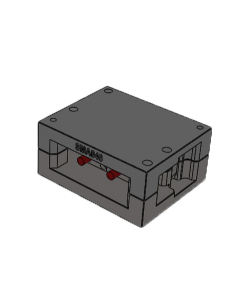
Low pressure moulding is an innovative technology made by using polyamide-based resins (e.g. TECHNOMELT ®). Through this process it is possible to encapsulate particularly fragile electrical and electronic components, making them more robust, insulated from external agents and ready to use. In fact, thanks to the low injection pressures, we can apply this process also on the main electronic components (both traditional and smd) on PCBs, without damaging them.


This moulding technique reduces the duration of the production
cycle, compared both to potting, which requires long curing times, and to traditional moulding, which involves subsequent assembly phases.
Through low pressure moulding the process will take just a few minutes to obtain a finished product ready for use. This process does not involve any additional step. In addition, you will spare time and money. Finally, you can obtain a precise design, which will result in minimizing the size and containing material costs.

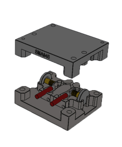
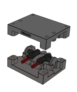
Placement of the PCB or other moulding device, moulding, removal
of the final product
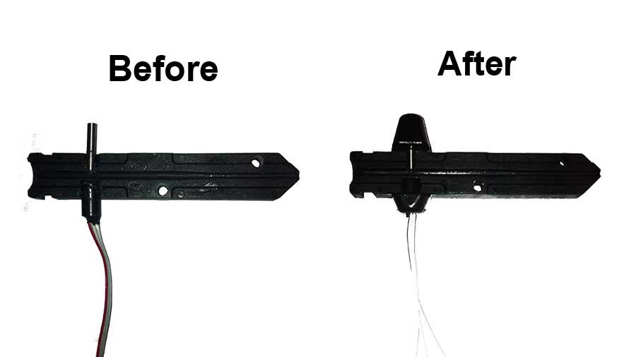
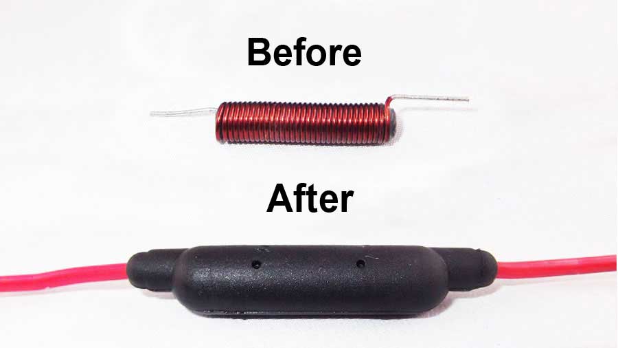
Moulded cable fairleads
This technology allows us to create custom-made cable fairleads . The end result is a bespoke finished product incorporated on the cable, thus, preventing any coupling that could generate infiltrations.
Main applications
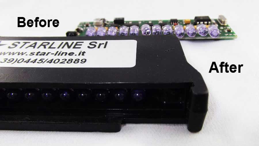
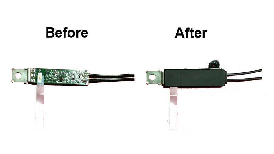
Insulation of PCBs and sensors
Thanks to the low injection pressures, it is possible to apply this process also on the main electronic components (both traditional and smd) on PCBs, without damaging them . The result is a ready to use and solid finished product, which is protected from external agents such as dust, water, humidity.
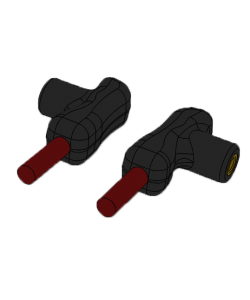
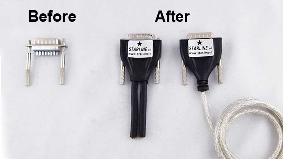
Moulded connectors
Technomelt resins can also be used to mould connectors, thus offering the customer the highest degree of flexibility on finished products. By way of example, it is possible to transform printed circuit connectors into “cable” connectors , ensuring the insulation of side terminals on the cable.


Benefits of Hot-melt resins
![]()

![]()
![]()
![]()
![]()

Cost-saving technology
Simplified production process, optimization of cycle time reducing costs.
![]()
![]()
![]()
![]()
![]()
![]()

Our resins
![]()

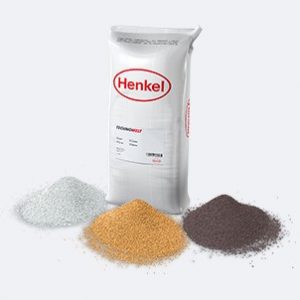
Technomelt ®
Technomelt ®Working with Henkel enables us to offer our customers moulding with Technomelt® Resins.
By using these resins we can obtain a finished product, which meets specific features including degrees of protection up to IP67.
Main features of Technomelt® resins:
![]()
![]()
![]()

Sustainability
Technomelt® Resins are environment-friendly
![]()
![]()
![]()
![]()
![]()